Microelectromechanical Systems (MEMS) and Photonics Devices

Micro-Nano Rapid Prototyping

L3Harris process engineers working at government-funded state-of the-art cleanroom facilities provide the unique ability for inexpensive fully in-house rapidly developed solutions from chip-level die design to wafer-level packaging. Turnaround time as quick as one week compared to foundry often requiring six months or more at three times the cost.
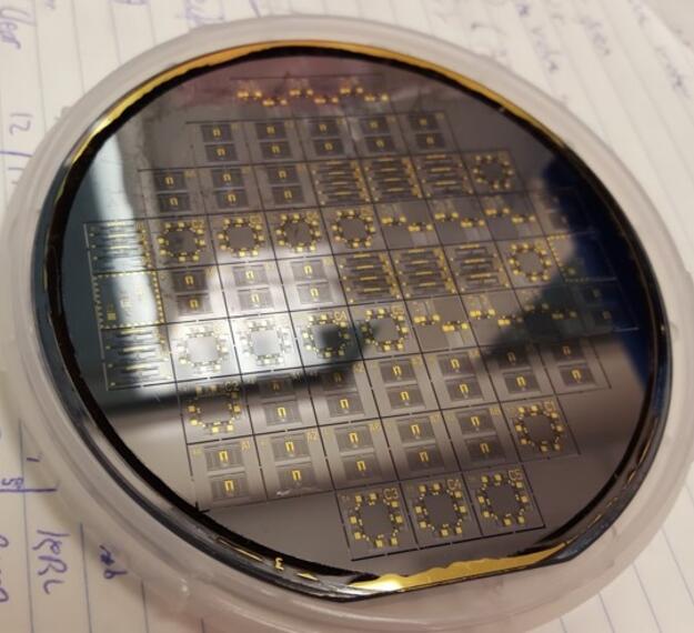
Semiconductor Microfabrication

  • Lithography
  • Metrology
  • Deposition
  • Dry etch
  • Wet etch
  • Atomic Layer Deposition
  • Thermal oxynitrides
  • Silicon
  • Si3N4
  • SiO2
  • SiC
  • 40+ metals E-Beam lithograph and processing
  • LiNbO3
  • InP
  • GaAs processing

Collaboration

The MPD group works with other scientists and engineers at L3Harris to introduce chip-level SWaP reductions to their systems. The group is available to help model and design microsystems and then develop the microfabrication processes needed to make the system a reality. It is also available to assist the photomask design and layout, multiphysics modeling or full system creation including water or chip microfabrication.


Benefits

  • On-site process engineers provide immediate feedback throughout fabrication
  • Fully in-house team enables rapid concept-to-test development cycles
  • 70-plus cutting edge microfabrication tools without the maintenance fees maximizes value
  • Photolithography mask creation, direct write lithography or E beam lithography enables a wide range of MEMS & photonic devices
  • Ability to process piece parts up to 200 mm wafer lots to accommodate one-off research and development projects up to low-rate initial production

Related Domains & Industries

Solutions that solve our customers' toughest challenges.
view all capabilities